Current research topics
- Dynamic in-situ nanomanipulation of van der Waals heterostructure devices (NSF Career Award)
- Study of ultrathin bismuth and other heavy metals via crystals grown between vdW materials (AFOSR)
- Chen, L., Wu, A.X., Tulu, N. et al. Exceptional electronic transport and quantum oscillations in thin bismuth crystals grown inside van der Waals materials. Nat. Mater. 23, 741–746 (2024). https://doi.org/10.1038/s41563-024-01894-0
- High-frequency gating and sensing of fluid transport through vdW heterostructure nanopores (DOE EFRC)
- Terahertz acoustic phonon amplification in graphene
- Quantum sensing with vdW Materials (UC Noyce Initiative)
Overview
We seek to discover new funky behaviors for electrons that have no counterpart in the world of classical physics.
Our strategy is to design strange landscapes for the electrons to live in and observe how they behave and interact with their neighbors. To accomplish this, we use advanced nanofabrication techniques as well as electronic, optical, and magnetic characterization methods.
Our end goal is to invent new useful quantum devices that manipulate charge, light, heat, spin, and information.
Let’s go into more detail of how this goes down:
Step 1: Confine electrons in 2-dimensions (2d)
Electrons normally live in 3 dimensions. We begin by shrinking down one of those dimensions so that it is smaller than the quantum wavelength of the electron. This makes quantum effects more obvious, by limiting the degrees of freedom.
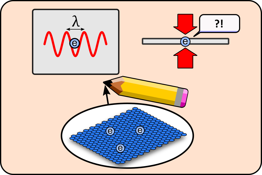
Instead of squishing down some material that contains electrons, we instead use a material that is intrinsically 2-dimensional. We get this from a 2d layered material
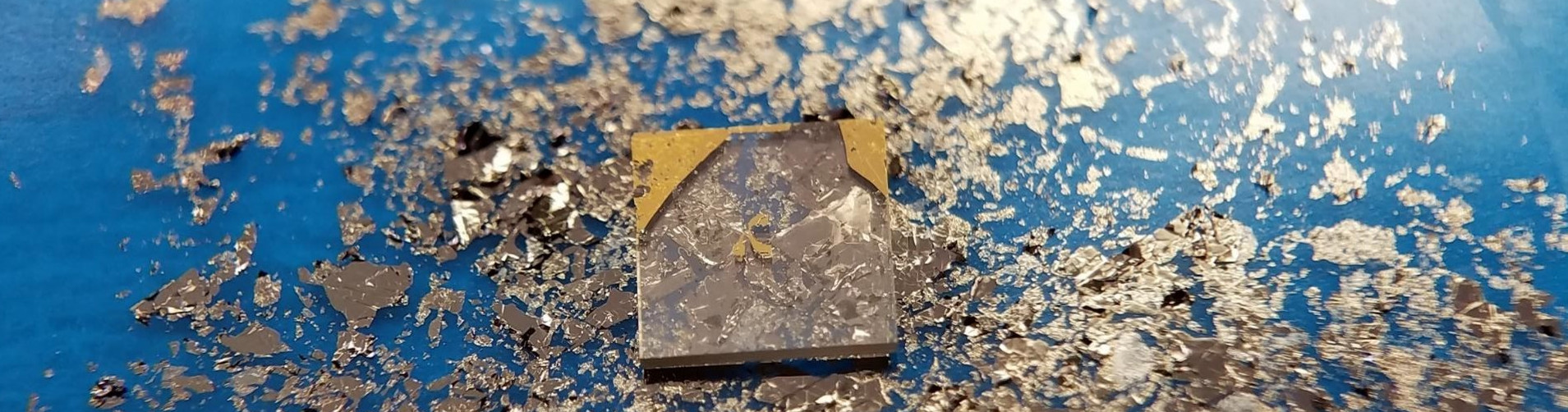
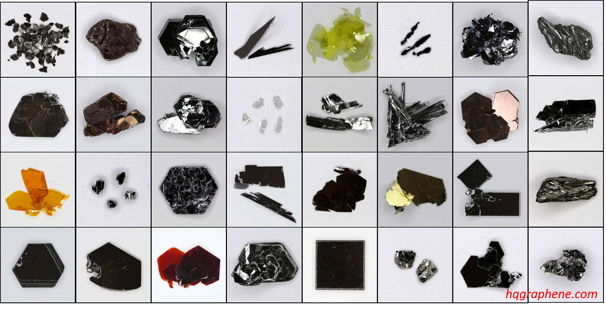
2d layered materials are made up of a stack of … layers! Each individual layer is made up of atoms connected by strong covalent bonds. Layers stick to each other via weak van der Waals forces, so they can easily slide across each other or even be peeled apart. The way we do this in the lab is by using Scotch tape (seriously).
The most famous 2d layered material is Graphite. A single layer of graphite is called graphene. So by isolating a piece of graphene, you can easily get a 2-dimensional playground for electrons!
| Learn more: Andre Geim and Konstantin Novoselov, winners of the 2010 Nobel prize for the discovery and isolation of graphene (lecture link here) |
Graphite and graphene are just the first examples of what we now know is a broad material class. In only the last couple of years, a diverse range of 2d layered material have been studied, including: metals, insulators, semiconductors, magnets, superconductors, topological insulators, strongly correlated materials, and .. this list keeps growing! For the first time, we can now study materials that have all of these different properties, but are also in the 2-dimensional limit.
In the 2d limit, electrons behave very differently than they do in the 3d version of the material. This is a very active area of research. For example, it was recently discovered that if the material WTe2 is thinned down to a single monolayer, it changes from being a semi-metal to having both a superconductor and topological insulator phase. When electrons go superconducting, they can carry a current with zero resistance, this is fundamentally a very quantum effect! A topological insulator is a special form a matter where the boundaries of a material are metallic, while the interior is insulating. To get both effects in the same material is awesome.
Step 2: Engineer the landscape for the electrons
As mentioned above, it already is interesting to study materials in the 2d limit. But, this is just the beginning! A monolayer of a 2d material can now serve as building block for engineering an entirely new material from the ground up. For the same reasons that allow 2d layered materials to be peeled apart, different 2d layers can also be recombined by stacking to make a 2d material heterostructure (also called Van der Waals heterostructure).

We have immense freedom in the combinations of materials that we can stack together in these heterostructures. Things get really interesting if the combined materials have different properties, because coupling between the layers causes hybrid effects. For example, what happens when we combine a ferromagnet with a superconductor? Or a material with strong spin-orbit coupling with a semi-metal? Can we build up an entirely new 3d material via stacking that still displays many of the behaviors of a 2d material?
| Read more: “2D materials and van der Waals heterostructures” |
Stacking allows us to engineer properties in the z-direction, but it is also interesting to modify the electronic landscape in the x-y plane of the layer.
The stacking method offers a beautiful method to do this. You see, when two different periodic lattices are superimposed, a new super structure emerges called the moire pattern. The length scale of the moire can be much larger than the original lattices, and can be controlled by twisting one layer with respect to the other. This gives us a great knob to control the environment for the electrons.
The twist-controlled moire does more than just create pretty pictures, it can dramatically change the quantum electronic behaviors of the electrons in a material. In the presence of a magnetic field, the moire length scale competes with the confining effects of the magnetic field leading to an incredible fractal energy structure known as Hofstadter’s butterfly. Things get even crazier if the electrons are forced to interact with each other in such a structure. Recently, it was demonstrated that twisted bilayers of graphene exhibits strongly correlated physics similar to high-temperature superconductors, including both a Mott insulator-like phase and a low-density superconducting phase.
This is an exciting time for this young field. There is both a wide variety of materials to be studied and an unlimited number of combinations to explore with heterostructures.
(more to be added soon!)
Are you a UCI student and interested in learning more?
Get in contact with the PI!
research keywords:
- graphene
- 2d layered materials / van der Waals heterostructures
- diamond NV nano-magnetometry
- nanofabrication
- photonics
- topology
- strongly correlated electrons
- emergent phenomena
- Driven non-equilibrium dynamics
- metamaterials
- Materials that compute